Browser-based electronics workflow

Online PCB design software.One project from schematic to board.

Struct is browser-based PCB design software that keeps the editable schematic, synchronized board layout, routing, parts, ERC, DRC, 3D review, manufacturing setup, and generated files in one controlled electronics project.

  • Schematic-to-PCB sync
  • Manual + automatic routing
  • ERC + DRC
  • Gerber + drill outputs
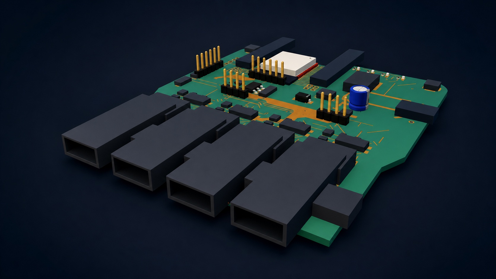
PCB · synchronized 3D reviewRendered from editable board data
Interactive PCB review in Struct showing the board outline, copper routing, footprints, connectors, and mounted components

The 3D view follows current outline, placement, pad, hole, via, side, and stackup data; it is a review view, not mechanical sign-off.

Schematic-to-PCB workflow

Keep electrical intent and physical implementation connected.

Stable component, terminal, footprint, pad, and net identities let you update the board from the schematic, find both sides of a connection, and regenerate outputs from the current design revision.

01

Capture the circuit

Place editable components and pins, draw real nets, assign exact part and footprint identity, and run the modeled electrical rule check.

  • Independent pins and stable net identities
  • Junctions, buses, labels, and no-connects
  • Catalog parts and custom definitions
02

Lay out and route the board

Synchronize footprints without discarding placement, define the outline and stackup, then edit pads, tracks, vias, zones, keepouts, and graphics.

  • Up to ten editable copper layers
  • Manual routing and bounded autorouting
  • Through, blind, buried, and micro vias
03

Check and prepare outputs

Run DRC, inspect the board in 2D and 3D, review CAM and BOM evidence, and create fabrication, assembly, and editable-source packages.

  • Current-revision ERC and DRC evidence
  • Gerber, drill, BOM, and placement files
  • Checksummed package manifests

Native board editor

Edit the geometry engineers need to inspect.

Work directly with the physical board model instead of a flattened illustration. The saved design carries the authoritative outline, copper stack, placements, footprints, pads, drills, traces, vias, zones, keepouts, rule areas, artwork, and dimensions.

Editable PCB modelOne revision across views
Physical review2D layout + synchronized 3D

Locate the same part, connection, or finding without reconstructing context.

Copper
F.Cu to B.Cu
Checks
ERC + DRC
State
Revision-bound
  • 01Footprints and padsEdit reference, value, part identity, side, rotation, position, courtyard, pad shape, drill, plating, mask, paste, and thermal properties.
  • 02Tracks, vias, and copperRoute straight or curved copper, add through or controlled span vias, build zones, and preserve net identity through every edit.
  • 03Stackup and layersControl visibility, locking, active layer, copper roles, and dielectric construction from a two-layer board through ten copper layers.
  • 04Cross-view inspectionCross-probe footprints and pads to the schematic and review current board geometry in an interactive three-dimensional view.

Controlled manufacturing handoff

Generate files without confusing export with approval.

Struct separates modeled checks, CAM preflight, BOM review, supplier evidence, package integrity, and human release state so a ZIP or green local check is never presented as proof of manufacturability.

Use the PCB manufacturing files checklist →

01

Resolve the modeled checks

Run ERC and DRC against the current design fingerprint, locate findings on the source objects, and document any deliberate exception.

02

Inspect the generated files

Review copper, mask, paste, silkscreen, outline, plated and non-plated drills, slots, BOM, netlist, and pick-and-place records.

03

Verify the package independently

Open the CAM output in an independent viewer, reconcile the stackup and fabrication notes, and run the intended supplier's DFM process.

04

Release a named revision

Keep fabrication, assembly, and editable-source manifests separate, verify their checksums, and attach explicit approval to the exact controlled bytes.

PCB design software questions

What to verify before relying on the board outputs.

Struct makes the captured design and its evidence reviewable. It does not infer missing electrical, mechanical, fabrication, assembly, test, or approval facts.

What is online PCB design software?+

Online PCB design software runs in a web browser and provides schematic capture, board layout, routing, verification, visualization, and manufacturing-file preparation. Struct keeps those views in one editable electronics project rather than splitting them across disconnected documents.

Can Struct synchronize a schematic with a PCB layout?+

Yes. Struct preserves stable component, terminal, footprint, pad, and net identities, reports pending schematic changes, updates PCB identity without disturbing approved placement, and supports cross-probing between schematic and board views.

How many PCB copper layers can Struct edit?+

Struct supports F.Cu, up to eight editable inner copper layers, and B.Cu, for a maximum of ten editable copper layers with explicit dielectric rows. The layer count is an editing capability—not approval of a particular material construction, impedance plan, manufacturer, or fabrication process.

Which PCB manufacturing files can Struct generate?+

Struct generates current-project Gerber layers, plated and non-plated drill data, slot data, a BOM, netlist, pick-and-place data, generated-output notes, and controlled review or release manifests. Reopen the files in an independent CAM viewer and complete supplier DFM before release.

Does a clean ERC or DRC make a PCB production-ready?+

No. ERC and DRC cover modeled electrical and geometric rules. They do not replace source verification, footprint approval, impedance or thermal analysis, independent CAM inspection, supplier DFM, testing, or named release approval.